
NEWS
Samsung’s HBM4 Doubling Starts With the Glass Carriers
Samsung’s 2027 HBM4 doubling shows up first as a 2.5 times jump in glass-carrier cleaning for 12-layer stacks.

Samsung Electronics plans to more than double HBM4-family output in 2027. Industry sources on September 20, 2026 are reading that ramp off a 2.5 times jump in glass-carrier cleaning, not off a matching rise in wafer starts.
The HBM4 family, sixth-generation HBM4 plus seventh-generation HBM4E, is the high-value mix Samsung wants at the center of its AI memory line. The first new order is for the glass plates that keep those wafers from cracking while they are ground thin.
Outsourced Cleaners Book 50,000 Sheets a Month
Those sources said Samsung will raise outsourced cleaning of glass carriers to 50,000 sheets a month in 2027 from 20,000 sheets a month in 2026. The same step ran at 10,000 sheets a month in 2025, so the wash load doubled once and is now set to rise another 2.5 times.
A glass carrier is a temporary glass support bonded under an HBM DRAM wafer so the slice does not bend or break while it is thinned and drilled. HBM4 and HBM4E are built around 12-layer stacks and higher, which is why the wash shops see the ramp before finished stacks leave Cheonan.
Analysts who track the step say carriers are reused after they are washed, and that use per wafer moves with yield and with how a line loads the process. Even after that, they read a 2.5 times jump in related volume as at least a doubling of HBM4 and HBM4E output from 2026.
THE SAMSUNG HBM RAMP IN FIGURES
| Measure | 2025 | 2026 | 2027 plan |
|---|---|---|---|
| Glass-carrier outsourced cleaning | 10,000 sheets/month | 20,000 sheets/month | 50,000 sheets/month |
| HBM wafer input, monthly average | – | about 180,000 | about 250,000 |
| HBM4-family share of HBM shipments | – | about 40% | about 80% |
Total HBM wafer input is projected to rise nearly 40 percent, from about 180,000 wafers a month in 2026 to about 250,000 in 2027. If the family mix moves from about 40 percent to about 80 percent on that larger base, HBM4-family wafer starts go from about 72,000 a month to about 200,000, a 2.78 times lift that matches the “at least twofold” reading.
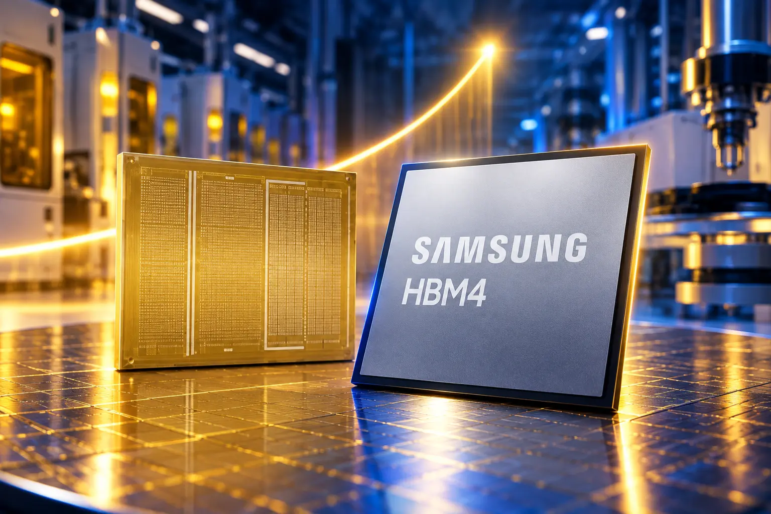
The Plate That Keeps a Thinned Wafer From Breaking
HBM has to stack several DRAM dies inside a fixed package height. As the stack count rises from eight layers to 12 and 16, each die has to come off the grinder thinner, and warp control starts to decide yield.
Industry estimates put the JEDEC thickness window for HBM4 near 775 micrometers. To fit 16 layers in that space, each chip is ground to around 30 micrometers, about one-third the thickness of a human hair. At that gauge a wafer behaves like paper that has been glued on one side: stress on one face curls the whole slice, and a single cracked die can scrap the stack.
Glass is used because its expansion rate is steady and the sheet can be made very flat. Corning, which sells temporary-bond carriers for wafer thinning and 2.5D/3D packaging, says its ultra-flat plates reduce warp by up to 40 percent in those flows. The glass is also clear, so a laser can bond and release it with less force than a mechanical peel, which cuts chip breakage on the way off the carrier.
This plate is not the glass substrate some packagers want under a whole GPU module. It is a shop-floor tool: bond, grind, drill, debond, wash, repeat. German specialty-glass firm SCHOTT has already sold borosilicate carriers into packaging lines as a stand-in for silicon carriers. Korean tool firms have built ultraviolet-laser bonders and debonders so the glass can come off without crushing the thinned DRAM.
Why Cleaning Volume Outruns Wafer Starts
The glass order grows 2.5 times while total HBM wafer starts grow nearly 40 percent. That gap is the tell. Extra cleaning is not a second copy of the same wafer plan; it is a heavier thinning load on each wafer that goes into a 12-layer or taller stack.
WHY THE GLASS ORDER RUNS AHEAD OF THE WAFERS
- Higher stacks: HBM4 and HBM4E center on 12-layer parts and above, so each DRAM wafer spends more time on the grinder and needs a carrier for that pass.
- Reuse, not scrap: Carriers are cleaned and reused after thinning, which is why wash volume can jump even when the glass is not thrown away.
- Yield still taxes the step: Early HBM4 mass production ran below 60 percent yield, and a failed thin wafer still consumes a carrier cycle.
- Starts are not shipments: A 250,000-wafer month in 2027 is input. Sellable HBM4E still has to clear customer tests, so some of that glass will be spent on parts that never ship.
If the extra glass were only a copy of today’s mix, cleaning would track the 40 percent rise in wafer starts. It does not. The wash shops are being sized for a line that thins more dies per finished stack, which is what a shift from older HBM into HBM4 and HBM4E looks like from the back end.
That is also why 2027 still feels tight for the accelerators that need the parts. A doubling of the family, booked on glass, is a capacity signal. It is not the same thing as finished stacks sitting in Nvidia’s bin.
Yield on the 1c Stack Has Reached About 80 Percent
Samsung began mass-production shipments of HBM4 in February 2026, using 10-nanometer-class sixth-generation (1c) DRAM and a base die from its own 4-nanometer foundry. The company said those first lots held a consistent 11.7 gigabits per second pin speed, with room to 13 Gbps, against a JEDEC mark of 8 Gbps.
Sang Joon Hwang, executive vice president and head of memory development, tied that spec to the node choice.
Instead of taking the conventional path of utilizing existing proven designs, Samsung took the leap and adopted the most advanced nodes like the 1c DRAM and 4nm logic process for HBM4.
Sang Joon Hwang, Executive Vice President and Head of Memory Development, Samsung Electronics
Industry sources now put HBM4 yield at about 80 percent, after a start below 60 percent. In a stacked product, a defect in one die can kill the whole cube, so that climb is what lets Samsung turn the same tools into more sellable parts. HBM4 is priced around 2 million won per chip, more than double fifth-generation HBM3E, which is why the mix shift is the earnings lever, not only the wafer count.
HBM4 ON THE LINE
- Early yield: Below 60 percent at the start of mass production in February 2026.
- Recent yield: About 80 percent on HBM4, with HBM4E above 70 percent at the reliability-evaluation stage.
- First revenue: Related sales cleared $1 billion (about 1.4 trillion won) within three months of those February shipments.
- Second-half mix: Samsung has projected that HBM4 will account for more than 60 percent of its HBM revenue in the second half of 2026, and that third-quarter HBM4 revenue will more than triple from the prior quarter.
The same February note said HBM sales would more than triple in 2026 from 2025, and that HBM4E sampling would start in the second half of 2026. Bandwidth per stack is listed at 3.3 terabytes per second, 2.7 times HBM3E, with 12-layer parts from 24 GB to 36 GB and a 16-layer path to 48 GB. Input/output count doubles from 1,024 pins to 2,048. Power efficiency is listed 40 percent better than HBM3E, with thermal resistance up 10 percent and heat dissipation up 30 percent.
Industry sources have also described new 1c DRAM lines at Pyeongtaek Line 4 sized at 100,000 to 120,000 wafers a month, dedicated to the DRAM that goes into HBM4. That is the front-end match for the glass order on the back end.
The 17-Point Gap With SK Hynix
Volume is also a share fight. Counterpoint Research put Samsung at 33 percent of global HBM revenue in the second quarter of 2026, up from 21 percent in the first quarter. SK Hynix stayed first at 50 percent, down from 58 percent. Micron held 18 percent, down from 21 percent.
GLOBAL HBM REVENUE SHARE, Q2 2026
| Supplier | Q1 2026 | Q2 2026 | Change |
|---|---|---|---|
| SK Hynix | 58% | 50% | -8 points |
| Samsung | 21% | 33% | +12 points |
| Micron | 21% | 18% | -3 points |
The gap between SK Hynix and Samsung shrank from 37 points to 17 points in one quarter. A year earlier, in the second quarter of 2025, Counterpoint had SK Hynix at 64 percent and Samsung at 15 percent. Most of that 2026 revenue was still HBM3E; Counterpoint said HBM4 shipments would show more clearly in the second half.
Samsung’s structure is the bet underneath those points. The 1c DRAM, the 4-nanometer base die, and the packaging sit in one company, so the three can be tuned together. SK Hynix has used TSMC for HBM4 logic dies, with a move toward a 3-nanometer-class die on HBM4E. That split is why a wash-shop order in Korea is also a foundry story: every extra HBM4 stack is another 4-nanometer base die from Samsung’s own line.
HBM4E Still Has to Clear Customer Qualification
The 80 percent mix figure for 2027 assumes HBM4E joins HBM4 in volume. That part is not done. Samsung sent 12-layer HBM4E samples to customers including Nvidia in May 2026, and yield at the reliability-evaluation stage is said to have moved above 70 percent. Mass-production timing still depends on those qualifications and on how much customers pull.
THE HBM4 FAMILY CLOCK
- February 12, 2026: Samsung begins mass production and commercial shipment of HBM4 on 1c DRAM and a 4-nanometer base die.
- May 2026: 12-layer HBM4E samples go to customers including Nvidia and enter product validation.
- Second quarter 2026: Counterpoint records Samsung at 33 percent of HBM revenue, with SK Hynix at 50 percent.
- September 20, 2026: Industry sources put 2027 glass-carrier cleaning at 50,000 sheets a month and HBM wafer input at about 250,000 a month.
- 2027: HBM4-family shipment mix is projected at about 80 percent, contingent on HBM4E clearing customer qualification.
Custom HBM samples, built to a buyer’s spec, are due to reach customers in 2027. Until HBM4E is signed off, the glass order is a bet that the thinning recipe which got HBM4 to about 80 percent can be copied onto the next stack. The cleaners will be busy either way. The stacks that come off those carriers will only count as a doubling if the customer tests say they can.

Kering’s Growing Houses Cannot Outrun a Shrinking Gucci

Studio Staff and Bitcoin Buyers Built the Eminem Leak Case

A Mutated H1N1 Strain Is Hitting Younger Immunity First

Albert Heijn Returns at One-Third as Rivals Take Share

Art Basel Paris Ends After One Public Day

Thameslink Will Pad 60,000 Ironing-Board Seats From 2027

How Tall Was Adolf Hitler Really? Debunking the Myth of his Height

Micron Sells the Memory Shortage as Five-Year Contracts

Royal Caribbean Sends Los Angeles Ships to Singapore and Brisbane

U.S. Forces Clear Hormuz Mines, Then Hit Minelayers Again
-
 NEWS2 months ago
Thameslink Will Pad 60,000 Ironing-Board Seats From 2027
-
 SCIENCE3 years ago
How Tall Was Adolf Hitler Really? Debunking the Myth of his Height
-
 NEWS2 months ago
Micron Sells the Memory Shortage as Five-Year Contracts
-
 NEWS2 months ago
Royal Caribbean Sends Los Angeles Ships to Singapore and Brisbane
-
 BUSINESS2 months ago
U.S. Forces Clear Hormuz Mines, Then Hit Minelayers Again
-

 BUSINESS2 months ago
Sweetmore Bakeries Buys Fantasy Baking for Bar Work
-

 BUSINESS2 months ago
L Catterton Installs a Kraft Heinz Operator at Kettle Cuisine
-

 NEWS2 months ago
CISA’s 100 Water System Hacks Hit One-Operator Plants